- 您现在的位置:买卖IC网 > Sheet目录3881 > PIC18F8585T-I/PT (Microchip Technology)IC PIC MCU FLASH 24KX16 80TQFP
2004 Microchip Technology Inc.
DS30491C-page 13
PIC18F6585/8585/6680/8680
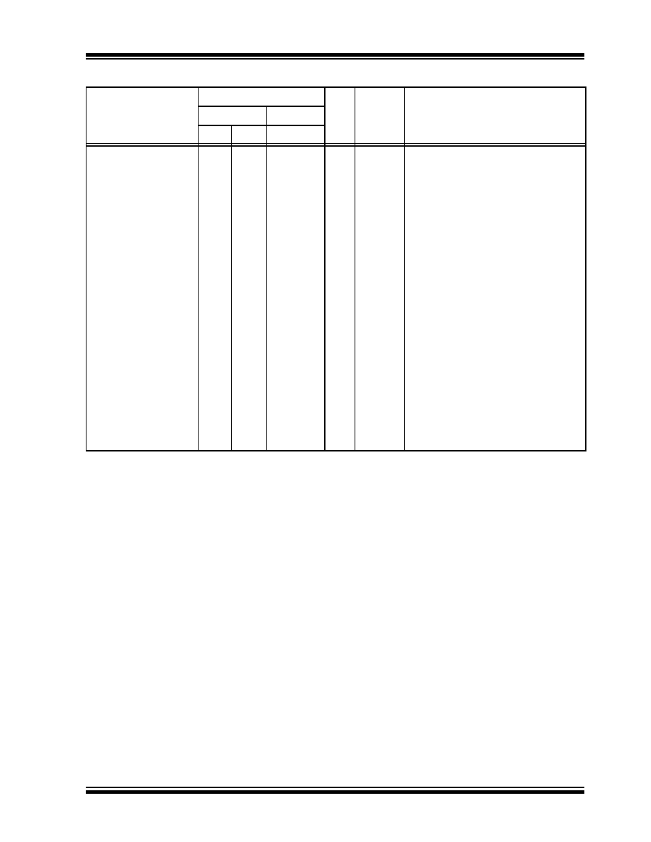
PORTA is a bidirectional I/O port.
RA0/AN0
RA0
AN0
24
34
30
I/O
I
TTL
Analog
Digital I/O.
Analog input 0.
RA1/AN1
RA1
AN1
23
33
29
I/O
I
TTL
Analog
Digital I/O.
Analog input 1.
RA2/AN2/VREF-
RA2
AN2
VREF-
22
32
28
I/O
I
TTL
Analog
Digital I/O.
Analog input 2.
A/D reference voltage (Low) input.
RA3/AN3/VREF+
RA3
AN3
VREF+
21
31
27
I/O
I
TTL
Analog
Digital I/O.
Analog input 3.
A/D reference voltage (High) input.
RA4/T0CKI
RA4
T0CKI
28
39
34
I/O
I
ST/OD
ST
Digital I/O – Open-drain when
configured as output.
Timer0 external clock input.
RA5/AN4/LVDIN
RA5
AN4
LVDIN
27
38
33
I/O
I
TTL
Analog
Digital I/O.
Analog input 4.
Low-voltage detect input.
RA6
See the OSC2/CLKO/RA6 pin.
TABLE 1-2:
PIC18F6585/8585/6680/8680 PINOUT I/O DESCRIPTIONS (CONTINUED)
Pin Name
Pin Number
Pin
Type
Buffer
Type
Description
PIC18F6X8X PIC18F8X8X
TQFP PLCC
TQFP
Legend: TTL
= TTL compatible input
CMOS
= CMOS compatible input or output
ST
= Schmitt Trigger input with CMOS levels
Analog = Analog input
I
= Input
O
= Output
P
= Power
OD
= Open-Drain (no P diode to VDD)
Note 1:
Alternate assignment for CCP2 in all operating modes except Microcontroller – applies to PIC18F8X8X only.
2:
Default assignment when CCP2MX is set.
3:
External memory interface functions are only available on PIC18F8X8X devices.
4:
CCP2 is multiplexed with this pin by default when configured in Microcontroller mode; otherwise, it is
multiplexed with either RB3 or RC1.
5:
PORTH and PORTJ are only available on PIC18F8X8X (80-pin) devices.
6:
PSP is available in Microcontroller mode only.
7:
On PIC18F8X8X devices, these pins can be multiplexed with RH7/RH6 by changing the ECCPMX
configuration bit.
发布紧急采购,3分钟左右您将得到回复。
相关PDF资料
XF2J-2424-11
CONN FPC 24POS 0.5MM SMT
PIC18LF6585T-I/PT
IC PIC MCU FLASH 24KX16 64TQFP
PIC18LF6680T-I/PT
IC PIC MCU FLASH 32KX16 64TQFP
XF2J-2224-11
CONN FPC 22POS 0.5MM SMT
PIC18F6525T-I/PT
IC PIC MCU FLASH 24KX16 64TQFP
PIC18F4439-E/ML
IC PIC MCU FLASH 6KX16 44QFN
XF2J-2024-11
CONN FPC 20POS 0.5MM SMT
PIC16LF747-I/ML
IC PIC MCU FLASH 4KX14 44QFN
相关代理商/技术参数
PIC18F85J10-I/PT
功能描述:8位微控制器 -MCU 32 KB FL 2 KB RAM RoHS:否 制造商:Silicon Labs 核心:8051 处理器系列:C8051F39x 数据总线宽度:8 bit 最大时钟频率:50 MHz 程序存储器大小:16 KB 数据 RAM 大小:1 KB 片上 ADC:Yes 工作电源电压:1.8 V to 3.6 V 工作温度范围:- 40 C to + 105 C 封装 / 箱体:QFN-20 安装风格:SMD/SMT
PIC18F85J10-I/PT
制造商:Microchip Technology Inc 功能描述:IC 8BIT MCU PIC18F 40MHZ TQFP-80 制造商:Microchip Technology Inc 功能描述:IC, 8BIT MCU, PIC18F, 40MHZ, TQFP-80
PIC18F85J10T-I/PT
功能描述:8位微控制器 -MCU 32 KB FL 2 KB RAM RoHS:否 制造商:Silicon Labs 核心:8051 处理器系列:C8051F39x 数据总线宽度:8 bit 最大时钟频率:50 MHz 程序存储器大小:16 KB 数据 RAM 大小:1 KB 片上 ADC:Yes 工作电源电压:1.8 V to 3.6 V 工作温度范围:- 40 C to + 105 C 封装 / 箱体:QFN-20 安装风格:SMD/SMT
PIC18F85J11-I/PT
功能描述:8位微控制器 -MCU 32KB Flash 2048BRAM 67I/O RoHS:否 制造商:Silicon Labs 核心:8051 处理器系列:C8051F39x 数据总线宽度:8 bit 最大时钟频率:50 MHz 程序存储器大小:16 KB 数据 RAM 大小:1 KB 片上 ADC:Yes 工作电源电压:1.8 V to 3.6 V 工作温度范围:- 40 C to + 105 C 封装 / 箱体:QFN-20 安装风格:SMD/SMT
PIC18F85J11T-I/PT
功能描述:8位微控制器 -MCU 32KB Flash 2048bytes-RAM 67I/O RoHS:否 制造商:Silicon Labs 核心:8051 处理器系列:C8051F39x 数据总线宽度:8 bit 最大时钟频率:50 MHz 程序存储器大小:16 KB 数据 RAM 大小:1 KB 片上 ADC:Yes 工作电源电压:1.8 V to 3.6 V 工作温度范围:- 40 C to + 105 C 封装 / 箱体:QFN-20 安装风格:SMD/SMT
PIC18F85J15-I/PT
功能描述:8位微控制器 -MCU 48 KB FL 4 KB RAM RoHS:否 制造商:Silicon Labs 核心:8051 处理器系列:C8051F39x 数据总线宽度:8 bit 最大时钟频率:50 MHz 程序存储器大小:16 KB 数据 RAM 大小:1 KB 片上 ADC:Yes 工作电源电压:1.8 V to 3.6 V 工作温度范围:- 40 C to + 105 C 封装 / 箱体:QFN-20 安装风格:SMD/SMT
PIC18F85J15T-I/PT
功能描述:8位微控制器 -MCU 48 KB FL 4 KB RAM RoHS:否 制造商:Silicon Labs 核心:8051 处理器系列:C8051F39x 数据总线宽度:8 bit 最大时钟频率:50 MHz 程序存储器大小:16 KB 数据 RAM 大小:1 KB 片上 ADC:Yes 工作电源电压:1.8 V to 3.6 V 工作温度范围:- 40 C to + 105 C 封装 / 箱体:QFN-20 安装风格:SMD/SMT
PIC18F85J50-I/PT
功能描述:8位微控制器 -MCU 32KB Flash 3936byte RAM RoHS:否 制造商:Silicon Labs 核心:8051 处理器系列:C8051F39x 数据总线宽度:8 bit 最大时钟频率:50 MHz 程序存储器大小:16 KB 数据 RAM 大小:1 KB 片上 ADC:Yes 工作电源电压:1.8 V to 3.6 V 工作温度范围:- 40 C to + 105 C 封装 / 箱体:QFN-20 安装风格:SMD/SMT